|
|
|
The circuit was derived at the logic level from its truth table shown
below:
|
|
|
|
|
|
|
|
|
|
|
|
|
|
|
|
|
|
|
|
|
|
|
|
|
A and B are the inputs to the system with Out representing the output of the nand gate.
The truth table was used to make a Karnaugh map which would provide
a simplified expression for the output.
B
|
|
|
|
|
A
0
|
|
|
|
1
|
|
|
I further realized that a nand gate is comprised of a pull-up network
and pull-down network. The pull-up network consists of two active
low (PMOS) transistors in parallel. The pull-down network consists
of two active high (NMOS) transistors in series. This situation is described
below in the image of the schematic. The inputs consist of square
waves to show the proper nand gate characteristics in the following simulation
output. The output of the circuit is an LED (Light Emitting Diode)
to show when the output is high (red) or low (black).

The Simulation Output:
The timing waveforms below show the proper functionality of the nand gate described by the truth table shown above. It can be seen in the waveforms that the output is low only when the two inputs are high, otherwise the output is high.
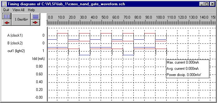
Note: The power dissipation is zero because you can not specify
the lengths and widths of the transistors in the Dsch program. Transistors
only act as switches in this program.
Calculations of transistor sizes:
To calculate the transistor sizes, the lab specifications needed to be taken into consideration. The nand gate needed to be able to drive 32 minimum cmos inverters (Wn=.3um, Wp=.6um) and 50fF of lumped wiring capacitance. The propagation delay needed to be less than 300ps using 50ps rise and fall times for the inputs.
The following steps were taken:
First, the load of the 32 cmos inverters in terms of capacitance was
needed.
CL = CW
+ CG
CG = (Number of Gates)*(Cap + Can) = N*(Cox*Wp*Lp + Cox*Wn*Ln)
| Cox = 9.3 fF/um2 | N = 32 | Ln=Lp=.2um | Wn=.3um | Wp=.6um |
Now that we have figured out the capacitive load, the transistor widths can be found by knowing the propagation delay. A propogation delay of 250ps was chosen such that the transistor sizes would not be too large, which is the case when when propogation delays become small.
tpHL and tpLH are defined as the delay experienced
by a signal when passing through a gate. They are measured between
the 50% transition points of the input and output waveforms. tpHL
corresponds to a high to low transition. Similarly, tpLH corresponds
to a low to high transistion. The propagation delay of a gate is
denoted tp and defines how quickly it responds to a change at
its input. tp is related to tpHL and tpLH by
the equation: tp = .5 ( tpLH + tpHL
) .
In the transition from high to low the output capacitance is discharged.
The worst case for tpHL is when both nmos transistors are on.
This situation can be described with the following equation.
tpHL =
CL*VDD
.5*kn*Wn*(VDD - Vtn)
In the transition from low to high the output is charged. The
worst case for tpLH is when only one pmos transistor is on. This
situation can be described by the following equation.
tpLH =
CL*VDD
kp*Wp*(VDD - |Vtp|)
| CL=.103pF | tpHL=250ps | tpLH=250ps | VDD=1.8V | Vtn=.4V | Vtp=-.42V | kn=275A(m-V) | kp=105A(m-V) | W=? |
Wn = 3.85 um
Wp = 5.12 um
A table comparing tpHL, tpLH, tp of the simulation and the hand calculations (for worst case).
Values of tpLH and tpHL were chosen to be 250ps such that the propagation delay would meet the desired specification of tp < 300ps and the transistor width would be small enough to fit in the 100 lambda cell height. The propagation delay was chosen to be close to 300 ps so that the transistor widths would be small, recalling that transistor width is inversely proportional to the propagation delay. tpLH and tpHL were assumed to be 250ps in hand calculations (that is how Wn and Wp were determined).
tp = .5 ( tpLH + tpHL )
| Hand Calculations | Simulation Results | |
| tpLH | 250ps | 87ps |
| tpHL | 250ps | 107ps |
| tp | 250ps | 97ps |
The Waveforms: indicating tpHL and tpLH (for worst case).
Below is the waveforms for the two inputs A and B to the nand gate and the output out1 of the nand gate. The following scenario provided the worst case for propagation delay. That is when A is high and B is switching to a high logic level or a low logic level. From the output waveform below, out1, you can see that tpLH is 87ps and tpHL is 107ps.
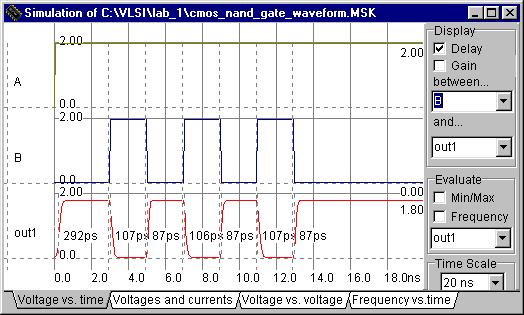
Note: tpHL = 107ps tpLH
= 87ps
The Layout: Indicating the size.
The image of the layout below is minimized as much as possible.
Height of the cell was specified to be 10um with the VDD and
GRD rails being 2um in height. In the image, the two nmos transistors
are in series to the left of the cell arranged vertically. To the
right is the two pmos transistors in parallel arranged horizontally to
minimize space. To create two nmos transistors in series, the diffusions
are shited to a side and another polysilicon line is added as the second
transistor. This is again done to minimize space. Also, to
create two pmos transistors in parallel the drain diffusions were shared
to minimize space and to reduce capacitance. A .103pF capacitance
was added to the output to represent the capacitive load of the 32 cmos
inverters as well as the 50fF of lumped wiring capacitance. Also,
the n-well for the pmos transistors is stretched into the VDD
rail to tie the well voltage to VDD.

The measuring rulers on the schematic show that the height of the cell is 10um while the width is 11.3um (shown as dx=113 lambda on the bottom of the schematic where lambda=.1um).
The simulation Output:
Below is the simulation of the output of the minimized nand gate. Notice that the output directly follows the truth table described above for a nand gate with the given input waveforms.
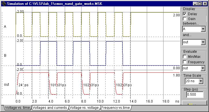
The waveforms: Indicating tpHL and tpLH ( for worst case ).
This is the simulation output of the minimized nand gate layout for the worst case input conditions. It was shown below that tpHL = 102ps and tpLH = 60ps. This implies a propagation delay of tp = 81ps.

* NOTE- on the out waveform above: tpHL = 102ps, tpLH
= 60ps
Static and Dynamic Power Dissipation.
From the simulation output of the layout, the total power dissipated in the system is 39.67uW (note: you can not see in the simulation output below since the window was made smaller for the web page). The waveforms below show the current of the gate with respect to time. Most of the current in the gate is due to dynamic power dissipation. The static power dissipation is due to leakage currents.
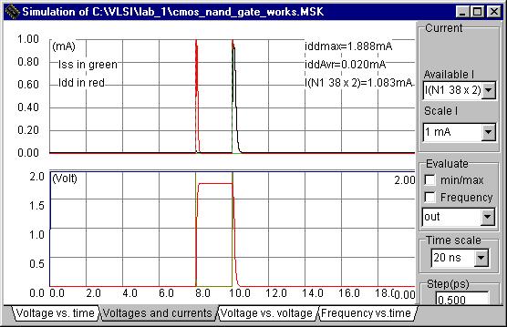
By knowing the average current Iddav=.02mA from the simulation
output above, the dynamic power dissipation can calculated using the equation
Pdyn = Vdd*Iddav = (1.8V)(.02mA) = 36uW. From
knowing the total power consumption and dynamic power dissipation you can
find the static power dissipation of 3.67uW using the equation Ptot
= Pdyn + Pstat.